Designing and manufacturing a Bionic Sensor
I spoke to Tim Constandinou about the Bionic Sensor he helped develop with a group of bionics researchers at the IBE. The chip is being used to test a range of technologies which might develop into different applications, including an artificial eye and pancreas.
The cost of manufacturing a microchip is expensive, so it makes sense to design a chip that can perform a range of experiments for individual researchers. As a result of this, the chip was designed to combine the research from fourteen individual projects. This page provides a short description of features of the chip then explores one of these projects in more detail - an imaging array for an artificial eye. The final section offers a description of the manufacturing of the chip.
Bionic vision is also the subject of Tim's thesis for the PhD he completed in 2005.

above: Tim demonstrating Cadence - an application that allows chips to be designed and tested, before being manufactured

above: The manufactured bionic chip is 5mm by 5mm, shown here on the tip of a finger
Some features of the bionic chip
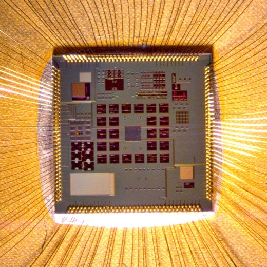
The image below shows the final design for the bionic sensor microchip. This is followed by a key describing the numbered reigons, which includes the names of researchers who designed the circuit in that reigon. This gives an idea of the range of research areas which make use of individual parts of the chip in laboratory experiments.
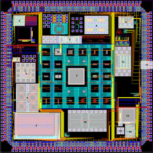
above: labelled regions of the bionic chip are described in the following key.
- 1 of 28 chemical sensors (ISFET-based) - Kostis Michelakis, Leila Shepherd, Pantelis Georgiou & Timothy Constandinou
- reference electrode (for chemical sensors) - Kostis Michelakis, Leila Shepherd, Pantelis Georgiou & Timothy Constandinou
- imaging array (alien vision project) - Timothy Constandinou & Patrick Degenaar
- filter for high frequency processing - Themis Prodromakis
- test photodiode structures - Dylan Banks
- new type of logic 1 (current-mode subtheshold) - Tor Sverre Lande
- new type of logic 2 (current-mode subtheshold) - Francesco Cannillo
- 5 ghz oscillators (4 of 6) - Sofia Vatti
- bichemical sensor interface (left interface hardwired to sensor and test pins, right wired to main pins) - Kritsapon Leelavatananon & Bhusana Premanode
- bichemical sensor sensor for interface above - Kritsapon Leelavatananon & Bhusana Premanode (left)
- bionic beta cell / artificial pancreas - Pantelis Georgiou
- chemical imaging array - Leila Shepherd
- colour aps imager - Francesco Cannillo & Timothy Constandinou
- edge detector based on mammalian retina (top) neuromorphic simple cell from the human visual cortex - V1 (bottom) - Dylan Banks
- floating gate for value storage - analogue flash memory - Patrick Degenaar
- bond pads linked to 4 chemical sensors - Kostis Michelakis
- ESD (electro-static discharge) protectors & buffers (to drive bigger wires and external features) between chips and us (blue) and pads to take wires (yellow)
The image sensor in more detail
The bionic sensor was designed in a platform called Cadence. This is a suite of complimentary applications that allow the chip to be drawn and tested. The images below are a sequence of screen-shots showing the layout of the bionic chip in Cadence. The initial shot shows the entire chip which is 5mm x 5mm, and the final shot shows an individual transistor which has features as small as 250nm x 600nm (L x W).
Dimensions are shown in millimetres (mm), micrometres (um) and nanometres (nm), and 1mm is equal to 1,000um and equal to 1,000,000nm. Read more about measurements of length from the National Physical Laboratory.
The whole chip (5mm x 5mm):
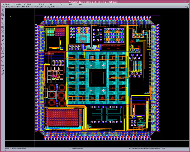
above: Cadence layout - a screen-shot showing the layout of the whole chip in the Cadence application.
The array (1.5mm x 1mm):
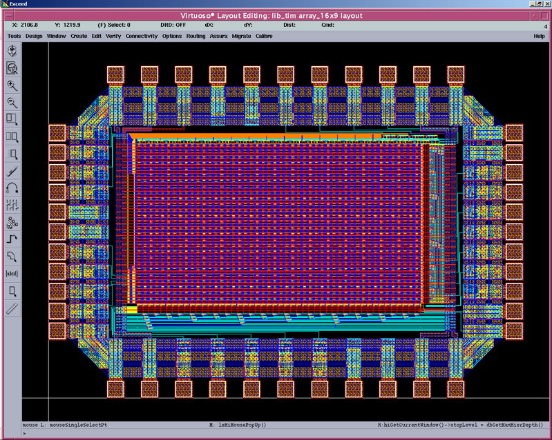
above: Cadence layout - zooming in on the image array in the bottom left corner, this like the CCD array in a digital video camera
A pixel group (150um x 150um):
![]()
above: Cadence layout - zoom in in further, here is a cluster of individual pixels on the large grid of pixels that make up the array
A single pixel (25um x 25um):
![]()
above: Cadence layout - zooming into the pixels, this is an individual pixel
A pixel transistor (250nm x 600nm):

above: Cadence layout - zooming into a single pixel, this transistor is one of the individual components of the pixel.
How the chip is manufactured
The final design is exported from Cadence as set of layers - a silicon chip is a 3-dimensional object, so these layers become transformed into a stack of metal and other materials when the chip is finally manufactured. The size of individual features of the chip are tiny. The bionic sensor was manufactured using a process that produced features of 250nm (nanometers). There are 1,000,000nm - or 1 million nanometers - in a millimetre. The thickness of a hair is about 100,000nm.
The chip was manufactured in 2005 with UMC. The clean factories that manufacture silicon chips are known as foundries. The foundry is sent the exported Cadence files and returns the completed chips. Each individual chip is cut by a diamond edged "micro-saw" from a wafer of silicon. Each silicon wafer can be made up of multiples of a single chip design, or many different chip designs. It's expensive to prepare the masks that are used to print the layers that make up the microchips. Once the masks are prepared, it is relatively cheap to print more wafers. A mask-set may cost up to $750,000 - $1,000,000. To help with the cost, IBE are a part of a group of universities called Europractice who combine their chip designs and share a small area of space on a multi project wafer, and benefit from an educational discount. 100 dies (separate chips) of the bionic sensor were produced in 2005, and are still being tested.
BBC news has a more detailed description of how silicon chips are made here, and here is an interactive animation of how a mask-set is used to build up different layers of material to make a silicon chip.
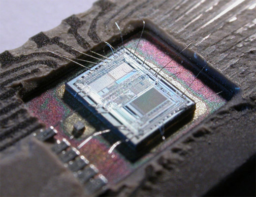
Once the chips are back in the lab, the square pads on the edge are connected by wires to larger and stronger pins, which attach to a socket in a circuit board. The pins are arranged on a standard form called a package - a 144 pin PGA package was used in this case, and there are total of 288 pads on the chip, so there were 2 variations of the packaged chip.
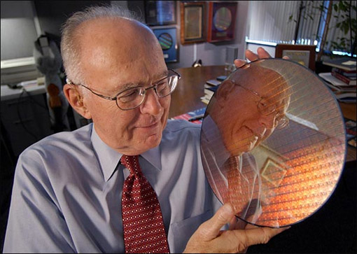
above: a wafer of silicon held by Gordon Moore, who with Moore's Law famously predicted that the amount of transistors on an integrated circuit would double every year (image from New York Times).
above: the bionic sensor chip with bond wires threaded to the pads on the edge.
above: A microchip is housed in a protective package, with the other end of the wires bonded to pins, which slot into a circuit board (this image from wikipedia shows a different chip).
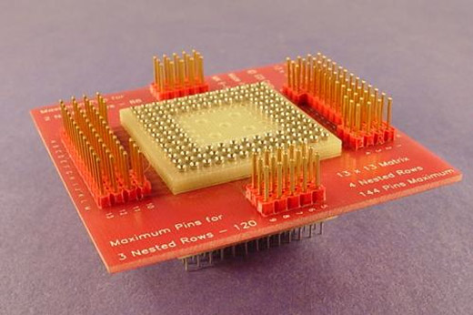
above: an example of the socket that the final package would clip into (image from www.logic-analyzer-adapter.com)
above: an image of the bionic sensor chip in an experiment to plate features with platinum to improve electrical conductivity
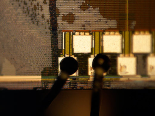
above: detail of two wires bonded to two of the pads on the bionic sensor chip
Interview by Tobie on 21st February 2008, all images by Tim Constandinou and Tobie Kerridge unless otherwise stated.